Sample work · Electronics
PCB design: IoT sensor board from specification to manufacturing data
A small sensor board with ESP microcontroller, USB-C and I²C interface: schematic, two-layer layout and manufacturing data in KiCad. Electrical and design rule check without errors, Gerber files re-imported.
Sample work (demo), not a client job. Built as a trial task with invented example data; the check figures below come from the automatic test run and are not polished.
What was built
- Schematic according to specification, components from the KiCad standard libraries
- two-layer layout, placement in code, connections with the autorouter
- ERC and DRC without errors; Gerber, drill data, bill of materials and component placement list
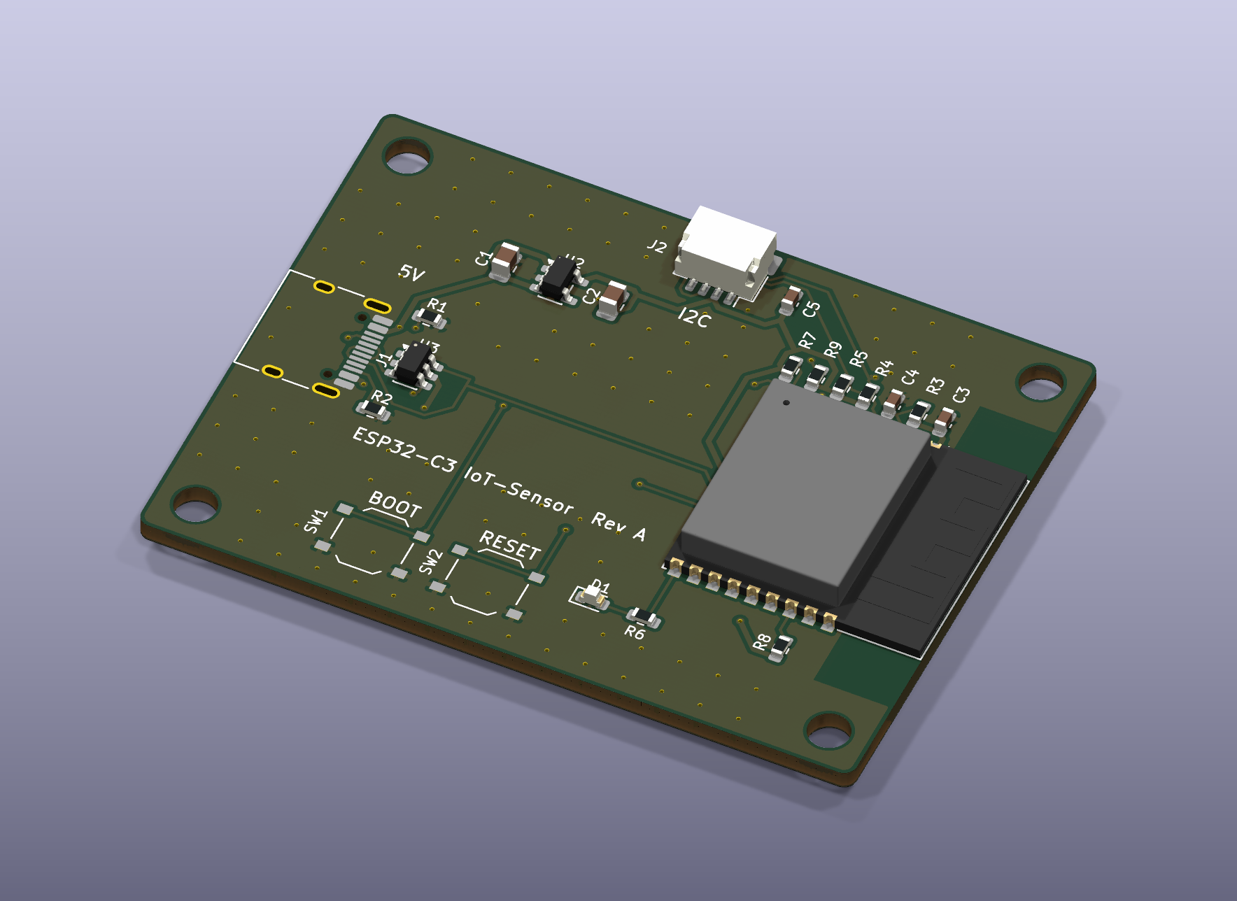
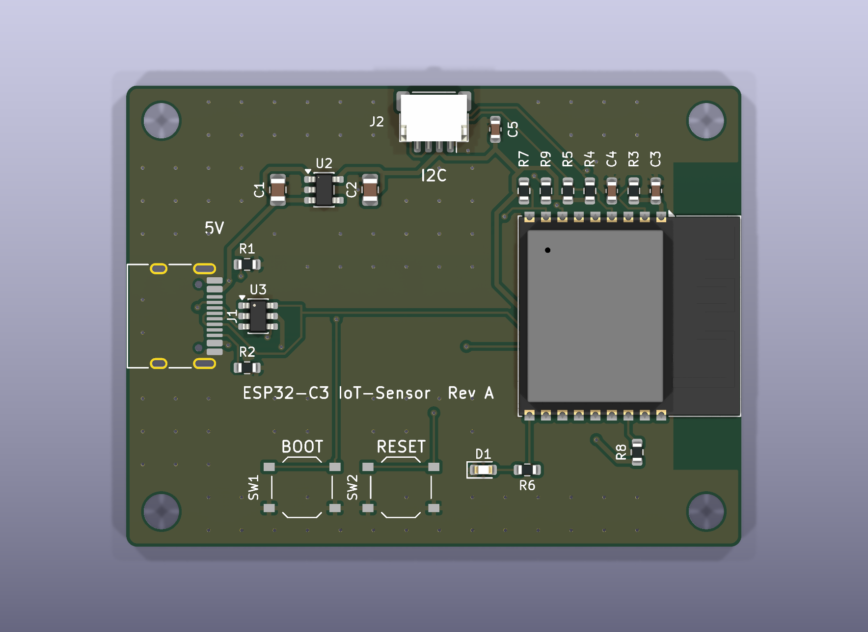
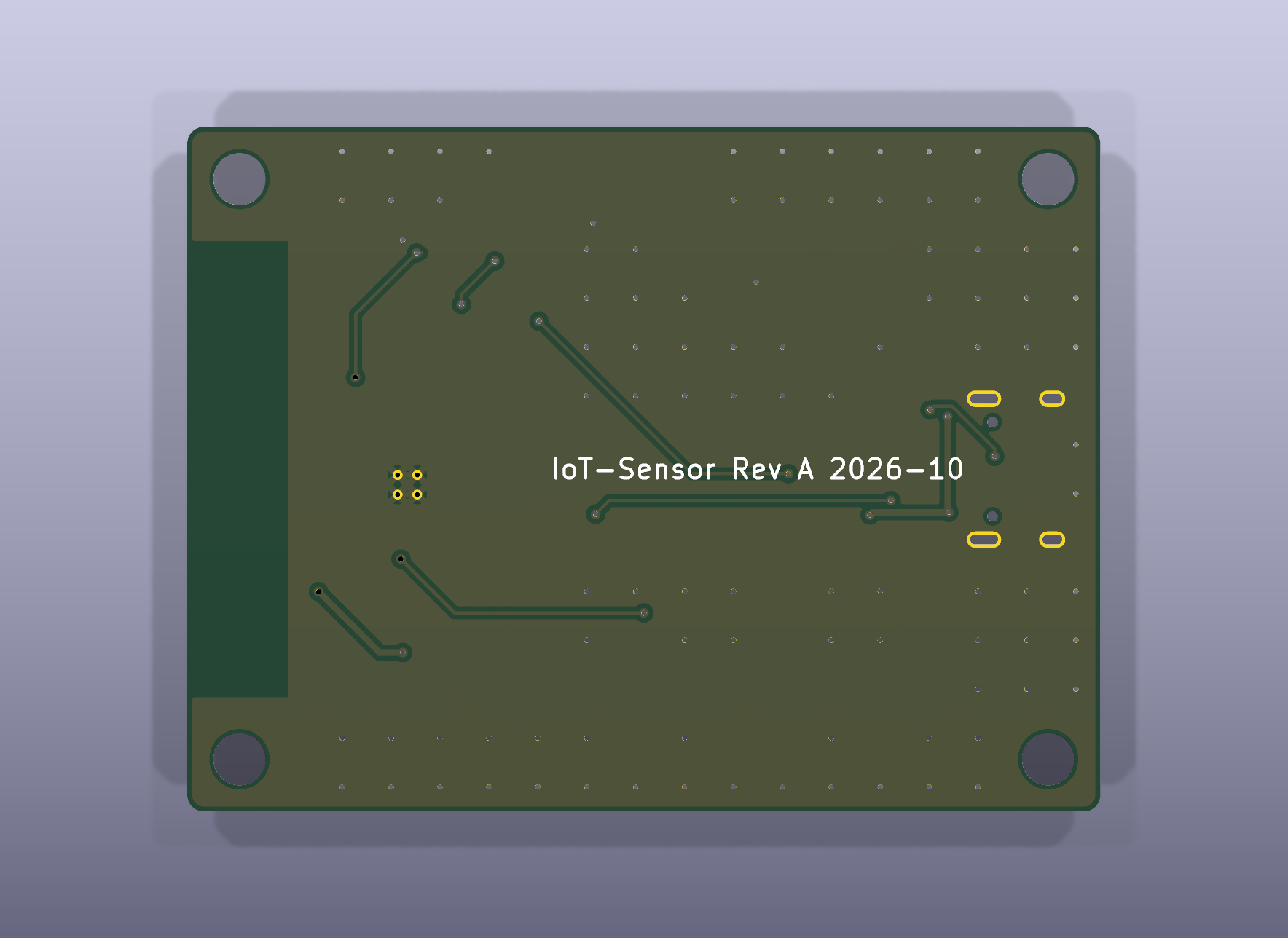
Download schaltplan.pdf Download fertigungsdaten-jlcpcb.zip
Demo without built board: verified are rules and datasheet circuitry, not a hardware test.
How it was checked
Automatic test run on 2026-10-31, taken from the log (test data invented, figures measured):
- 22 components, 15 nets according to specification
- ERC 0 errors/0 warnings
- DRC 0 errors/0 warnings, 0 unconnected, parity 0
- Gerber re-imported: outline 56.0 x 42.0 mm (target 56.0 x 42.0), 4 M3 holes at target position, 118 vias, 4907 track segments, 26 nets in copper
- BOM 15 rows/22 parts, CPL 22 positions
Limits
What this sample does not cover, so nobody expects more:
- Schematic, layout, DRC and manufacturing data (Gerber RS-274X2, Excellon, BOM, component placement list) with KiCad 10; project files .kicad_sch/.kicad_pcb are included - the customer can continue working in KiCad
- 2 layers (4 layers possible, not tested); digital and low-speed circuits: microcontrollers, sensors, I2C/SPI/UART, USB Full-Speed, voltage regulators, LEDs, buttons, connectors
- Autorouter (Freerouting) plus manual placement in code - no fine-tuning like from a layout designer working by the hour; differential pairs are not routed as pairs, no length matching
- No RF/antenna tuning (only finished radio modules with keep-out zone), no impedance control, no high-speed (DDR, PCIe, USB 3, Ethernet PHY layout), no power/high-voltage electronics …
- No certification (CE/FCC/UL), no EMC measurement, no firmware test on real hardware - functionality is verified by ERC/DRC and datasheet circuitry, not by a built board
- Footprints/symbols from KiCad standard libraries; components outside of those must be redrawn (costs time, no money). LCSC numbers are suggestions: availability and rotation angle …
- Schematic in net label style (blocks with labels instead of wire drawing) - electrically complete, visually simpler than a hand-drawn one
Something like this for your business?
Describe briefly what you need. You get a fixed price before I start; nothing happens without your yes.